A circuit can function correctly in simulation and still fail after it is manufactured.
Poor component placement, unsuitable trace widths, inadequate grounding, and missing manufacturing constraints can all create problems that are difficult to identify from a schematic alone.
PCB design software helps engineers translate an electrical circuit into a physical printed circuit board.
The right application should support the entire journey from circuit capture to manufacturing documentation, while making electrical and layout errors easier to detect.
What PCB Design Software Does
PCB design software is used to create the electrical and physical design of printed circuit boards.
A typical workflow begins with a schematic. The engineer selects components, connects their electrical pins, and checks the circuit.
The design then moves into PCB layout.
Components are placed on the board, electrical connections are routed, and manufacturing rules are applied.
The final design produces fabrication and assembly information that a manufacturer can use.
The PCB Design Workflow
Create the Schematic
The schematic defines the circuit’s electrical connections.
Component symbols must correspond to suitable physical footprints. Incorrect pin mapping can lead to boards that cannot function as intended.
Define the Board
The designer selects the board outline, layer stackup, materials, and manufacturing constraints.
These decisions influence routing, signal integrity, thermal performance, and production cost.
Place Components
Component placement affects electrical behavior and assembly.
Sensitive analog circuits, high-speed signals, power components, and connectors may require particular placement strategies.
Route Connections
Routing connects component pads using copper traces and vias.
Engineers must account for trace width, spacing, return paths, impedance requirements, and other electrical constraints.
Run Design Checks
Design rule checking helps identify violations of defined physical constraints.
Electrical rule checking helps detect selected schematic connectivity problems.
Passing these checks is necessary but does not guarantee correct electrical performance.
Prepare Manufacturing Outputs
Fabrication data commonly includes Gerber files and drill information, although other formats may be supported.
Assembly workflows may also require a bill of materials, placement files, and drawings.
PCB Design Software Options
Altium Designer
Altium Designer is a professional PCB design environment supporting schematic capture, board layout, and engineering documentation.
It is relevant to organizations managing complex PCB projects and collaborative engineering workflows.
Teams should examine licensing, design data management, and the advanced capabilities included in their selected package.
KiCad
KiCad is an open-source PCB design suite.
It supports schematic capture, PCB layout, design checks, and manufacturing outputs.
It is an attractive option for engineers who want a capable design environment without commercial licensing costs.
Autodesk Fusion Electronics
Fusion Electronics provides electronic design capabilities within the Autodesk Fusion environment.
It is particularly relevant when electronics and mechanical enclosure development need to be coordinated.
Cadence OrCAD X
OrCAD X supports PCB design workflows including schematic development and board layout.
It is worth evaluating for professional engineering teams that require structured design processes and related analysis capabilities.
Siemens Xpedition
Xpedition targets advanced PCB design workflows.
It is relevant to organizations dealing with complex board designs, engineering collaboration, and demanding manufacturing requirements.
EasyEDA
EasyEDA provides browser-oriented electronic design capabilities.
It can be useful for rapid development and projects that benefit from connected component and manufacturing services.
Users should assess project portability, data management, and the features available under their chosen plan.
PCB Design Software Comparison
| Software | Main Strength | Suitable Projects |
|---|---|---|
| Altium Designer | Professional PCB development | Commercial electronics |
| KiCad | Open-source PCB design | Education and professional projects |
| Fusion Electronics | Electronics and mechanical design coordination | Integrated product development |
| OrCAD X | Structured PCB engineering | Professional hardware teams |
| Siemens Xpedition | Advanced PCB workflows | Complex enterprise projects |
| EasyEDA | Accessible connected design workflow | Prototyping and smaller projects |
What to Evaluate Before Choosing
Board complexity: A simple two-layer board has different requirements from a dense multilayer design.
High-speed capabilities: Projects involving controlled impedance, differential pairs, and demanding signal integrity need appropriate constraint and analysis workflows.
Component libraries: Verify symbol and footprint quality. Poor library management can introduce serious manufacturing errors.
Mechanical integration: Check whether the software can exchange board geometry with the mechanical CAD system used for the enclosure.
Collaboration: Multiple engineers may need controlled access to shared libraries, revisions, and design files.
Manufacturing outputs: Confirm that the application can generate everything required by the selected fabrication and assembly partners.
Common PCB Design Mistakes
One frequent mistake is treating the design rule checker as a complete validation system.
A board can satisfy spacing rules while still suffering from noise, poor return paths, or thermal problems.
Another mistake is relying on component footprints without checking them against manufacturer documentation.
Engineers should also review board stackup, connector orientation, test access, and assembly requirements before releasing a design.
How to Test PCB Design Software
A useful evaluation project should include more than a simple demonstration circuit.
Select a representative board with realistic components and constraints.
Create the schematic, build the layout, run checks, export manufacturing files, and review the output with a fabrication partner.
If the team regularly designs enclosures, test the mechanical integration process as well.
This exercise reveals limitations that feature comparisons often miss.
Conclusion
PCB design software connects electronic ideas with physical manufacturing.
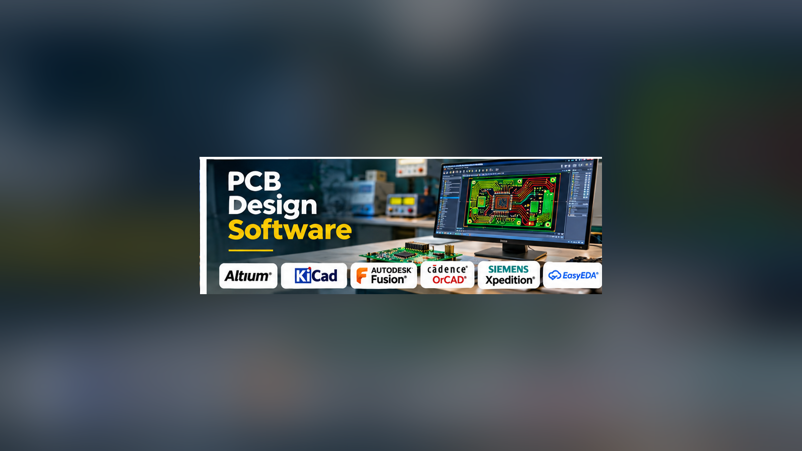
Altium Designer, KiCad, Fusion Electronics, OrCAD X, Xpedition, and EasyEDA offer different approaches to that process.
The most suitable choice depends on board complexity, collaboration needs, manufacturing requirements, and available engineering resources.
A reliable PCB workflow combines appropriate software with careful component selection, layout practices, electrical validation, and manufacturing review.